
Key facts
- The ceremony was attended by CEO Kwak Noh‑jung, K‑SURE officials, and representatives of KB Kookmin, Shinhan, Woori and Hana banks.
- The Export Supply Chain Strengthening Guarantee was signed at SK Hynix's Yongin Cluster exhibition center in Gyeonggi Province.
- Without qualification data, lenders cannot accurately price credit risk, so they over‑discount it or decline entirely.
- Qualifying MCE suppliers receive loan limits raised 50% above those offered to other industries under standard K‑SURE programs.
The guarantee program forms part of the government’s initiative to reinforce export supply chains by easing financing for smaller suppliers of major manufacturers. Earlier, the government committed 2.4 trillion won in loan guarantees to the automotive, shipbuilding and steel sectors before launching the semiconductor support. Industry Minister Kim Jung‑kwan said the government aims to expand chip‑sector financial support to over 5 trillion won and to boost research, investment and workforce training.
At the ceremony, qualifying suppliers received the first guarantee certificates.
Industry Ministry officials described the accord as the biggest trade‑finance arrangement ever made with a sole company. Minister Kim urged faster growth of domestic semiconductor output, noting that construction safety should stay a top concern.
Firms that are small or medium‑sized and provide specialty gases, photoresists, CMP polishing compounds, deposition equipment or inspection tools usually run on thin balance sheets and face restricted credit. If SK Hynix speeds up its expansion, supplier order books may grow faster than their available working capital. A Korean maker of a new photoresist for SK Hynix’s upcoming HBM cannot secure a development loan from a bank, as the bank lacks a way to test if the material meets SK Hynix’s qualification standards. To qualify, suppliers must spend time on a live production line that replicates mass‑production conditions. Without qualification data, lenders cannot accurately price credit risk, so they over‑discount it or decline entirely. This chicken-and-egg issue is the structural gap that the two‑part program unveiled on Monday aims to address.
Grasping the importance of the MCE supplier ecosystem starts with knowing what makes up a High Bandwidth Memory chip, central to South Korea’s AI‑driven hardware strength. The MCE suppliers protected by the guarantee program are the upstream companies that produce the materials enabling SK Hynix’s scale. HBM is a three‑dimensional memory architecture where multiple thin DRAM silicon dies are stacked vertically and connected through thousands of microscopic TSVs that run through the layers like vertical wire bundles. The HBM stack is placed on a silicon interposer next to the host processor — usually an Nvidia GPU or a hyperscaler’s AI accelerator — enabling data bandwidth unattainable with conventional flat 2D memory.
HBM3E delivers about 1,229 GB/s per stack, and an eight‑stack configuration provides roughly 9.8 TB/s. SK Hynix pioneered HBM with AMD and now holds an estimated 53‑58% share of the global HBM market. SK Hynix’s HBM dominance rests on successive generations of process refinement, with each new generation demanding a fresh cycle of materials and equipment qualification. CMP polishing compounds used to flatten each HBM layer must be re‑validated for each new generation, and etch gases used to drill TSV holes must perform consistently at the new geometries of each HBM generation. For each new HBM generation, photoresists that set circuit patterns must satisfy stricter specs, and qualifying suppliers need fab time they cannot obtain elsewhere for each qualification cycle.
SK Hynix holds about 70% of Nvidia’s HBM4 supply allocation for the Vera Rubin platform in 2026, according to analyst estimates. The company generated first‑half 2026 revenue of approximately $86.6 billion.
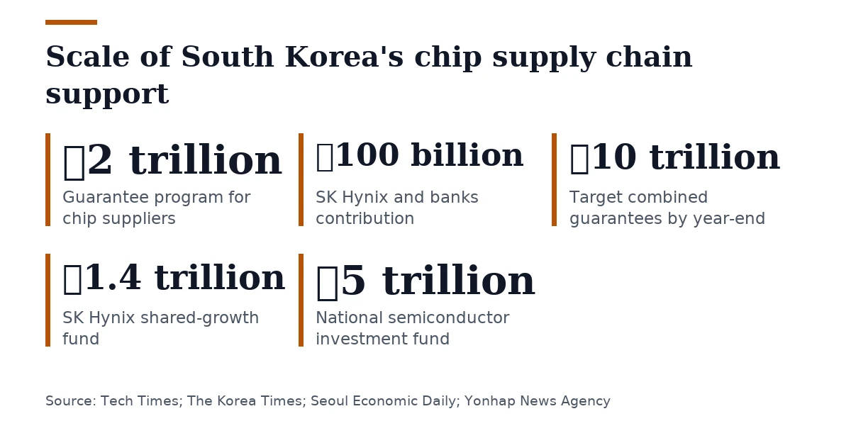
SK Hynix and four commercial banks put ₩100 billion (about $67 million) into the guarantee program, and K‑SURE boosts that amount twenty‑fold, enabling guarantees for as much as ₩2 trillion in supplier loans. Qualifying materials, components and equipment (MCE) suppliers receive loan limits raised 50% above those offered to other industries under standard K‑SURE programs, a guarantee ratio raised from 90% to 100% of the loan amount, an extended loan term of three years instead of one year, and interest‑rate cuts of up to 2.5 percentage points.
The guarantee fee, usually paid by the borrower, is cut by 25‑35% by K‑SURE, while the participating banks cover the remaining fee for the full three‑year term, and this mechanism is a formal instance of K‑SURE’s SMILE program — Supply‑chain Miracle by Leverage. In August 2025, the same SMILE structure backed ₩630 billion in guarantees for Hyundai Motor Group’s automotive suppliers after US tariffs disrupted that supply chain.
Extending the SMILE mechanism to semiconductors and nearly tripling its scale shows that Seoul regards chip supply‑chain fragility as a strategic priority on par with automotive disruption. The government plans to extend the guarantee program to defense, nuclear energy and biotechnology sectors, aiming for a combined ₩10 trillion in guarantees by the end of the year. The guarantee agreement signed on Monday is the largest and most formally structured part of SK Hynix’s 2026 support architecture for semiconductor suppliers, which it has been assembling since July.
In August 2026, South Korea’s government announced a ₩5 trillion national semiconductor investment fund targeting MCE and fabless companies. Moreover, the government pledged an extra ₩5 trillion for trade finance to suppliers and a ₩1 trillion supplier development program lasting ten years.
Signed on Monday, the K‑SURE guarantee acts as the private‑sector co‑investment component of the national semiconductor drive, allowing SK Hynix and the banks to share risk the national fund cannot cover alone. The announcement did not reveal the names of the first beneficiary companies or detailed qualification criteria, stating only that domestic MCE suppliers experiencing financing difficulty are eligible.
K‑SURE’s SMILE program in shipbuilding and automotive relies on large‑company recommendations to pick eligible suppliers, and the semiconductor version is expected to work the same way, with SK Hynix recommending partners to the banks and K‑SURE providing guarantees.
In July 2026, SK Hynix pledged to deploy ₩1.4 trillion (~$933 million) over five years in a shared‑growth fund to support MCE partner companies. In September 2026, SK Hynix moved up about ₩304.7 billion in supplier payments before the Chuseok holiday to relieve seasonal liquidity pressure. On September 29 2026, at the Partners Day event, SK Hynix introduced an R&D Challenge Reward System that will fund up to 50% of initial R&D costs for partner companies that have technical promise but limited capital. Payment under the R&D Challenge Reward System is settled regardless of commercial outcome, provided the technology meets agreed milestones. SK Hynix doubled its supply payment support fund, raising it from ₩50 billion to ₩100 billion (~$67 million). SK Hynix said it will offer consulting services to secondary and tertiary suppliers that were not previously covered by its support programs.
South Korea’s semiconductor export revenues reached a monthly record of over $60 billion in September 2026, accounting for about half of the nation’s total goods exports. South Korea’s semiconductor output still depends on a materials supply chain that was almost paralyzed in 2019 when Japan limited exports of hydrogen fluoride, fluorinated polyimide and photoresists, which had provided 70‑93% of Korean needs. Although localization efforts lowered dependence on Japanese sources, Korean MCE suppliers still lack the scale and financing needed to serve as reliable second‑source alternatives to Japanese, Dutch, and US providers of critical process materials.
In China, chipmakers such as YMTC and CXMT can mandate adoption of domestic materials and equipment by state policy, giving domestic products access to production environments without commercial negotiation. Chinese MCE developers do not need to produce qualification data to obtain financing, as the state can direct adoption before qualification is finished. South Korea cannot rely on administrative mandates to secure domestic semiconductor materials. SK Hynix, as a publicly listed company, makes procurement decisions based on commercial logic, requiring its chips to be the best available at acceptable cost to remain attractive to customers such as Nvidia.
The K‑SURE guarantee and Trinity Fab are market‑economy tools that offset the state‑ownership advantage by improving information and risk‑pricing conditions for semiconductor supplier financing.
Trinity Fab is a process‑demonstration facility of about 3,300 m² (≈35,500 ft²) under construction inside the Y1 fab building at the Yongin Semiconductor Cluster. Trinity Fab is financed by a joint investment of ₩870 billion (~$580 million) from the central government, Gyeonggi Province and SK Hynix. Trinity Fab provides MCE suppliers access to a real semiconductor manufacturing environment matching mass‑production conditions, allowing characterization and qualification of new materials and equipment without using commercial fab capacity.
SK Hynix describes Trinity Fab as infrastructure for technological independence. Attendees of the ceremony visited the Trinity Fab site and the nearby Y1 fab construction on Monday. The Y1 fab is scheduled to begin initial cleanroom operations in February 2027, pulled forward from an earlier May 2027 target. The Y1 fab aims to make sixth‑generation 10‑nanometer‑class (1c) DRAM and to support HBM4E, SK Hynix’s upcoming high‑bandwidth memory chip for AI accelerators. Trinity Fab is slated to begin operations in 2027.
Join the discussion